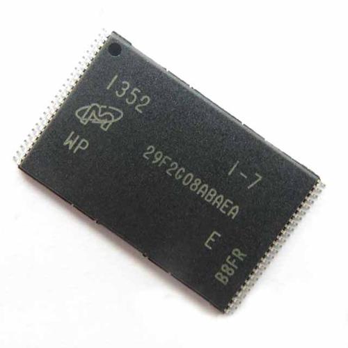
优势产品
 图片仅供参考,商品以实物为准
相似产品


MT29F128G08AJAAAWP-Z:A 详细参数介绍:
产品详情
| 脚位/封装 | TSOP-48 |
| 外包装 | |
| 无铅/环保 | 无铅/环保 |
| 电压(伏) | 2.7v-3.6v |
| 温度规格 | 0°C~+70°C |
| 速度 | 1 MHZ |
| 标准包装数量 | |
| 标准外箱 | |
| Number Of Words | 16G |
| Bit Organization | x8 |
| Density | 128G |
| Features | Polyimide (if applicable) |
| Package | TSOP I(48-pin CPL version) |
| Generation Feature Set | 1st set of device features |
| Speed Grade | Async only |
| Design Revision | A |
| Classification | 4-2-2-1 (Die-nCE-RnB-IO Channels) |
| Level | SLC |
| Production Status | Production |
| Package Material | Pb-free |
| Interface | Async only |
General Description Micron NAND Flash devices include an asynchronous data interface for high-performance I/O operations. These devices use a highly multiplexed 8-bit bus (DQx) to transfer commands, address, and data. There are five control signals used to implement the asynchronous data interface: CE#, CLE, ALE, WE#, and RE#. Additional signals control hardware write protection (WP#) and monitor device status (R/B#). This Micron NAND Flash device additionally includes a synchronous data interface for high-performance I/O operations. When the synchronous interface is active, WE# becomes CLK and RE# becomes W/R#. Data transfers include a bidirectional data strobe (DQS). This hardware interface creates a low pin-count device with a standard pinout that remains the same from one density to another, enabling future upgrades to higher densities with no board redesign. A target is the unit of memory accessed by a chip enable signal. A target contains one or more NAND Flash die. A NAND Flash die is the minimum unit that can independently execute commands and report status. A NAND Flash die, in the ONFI specification, is referred to as a logical unit (LUN). For further details, see Device and Array Organization.

热销产品
新闻资讯
深圳市时时发控股有限公司专营电子元件批发、电子元件采购,是综合性的电子元器件网上商城。
电子元器件商城主营:存储IC/内存条/SSD/HDD/CPU/GPU等,品牌包括:三星,镁光,海力士,英特尔,英伟达等。
© 2022 深圳市时时发控股有限公司 粤ICP备19078955号
网站地图


扫描二维码添加客服微信获取报价


 MTA32ATF4G64HZ-2G6B2 SODIMM DDR4 镁光


